In our increasingly interconnected world, the proliferation of electronic devices has brought unprecedented convenience. However, this technological boom comes with a silent yet significant challenge: electromagnetic (EM) radiation and interference (EMI). At FEHONDA, we understand the growing concerns surrounding EM pollution and the critical need for effective mitigation strategies. This guide delves into the fascinating realm of electromagnetic wave absorbing materials, exploring their research background, definition, performance evaluation, and differentiation from EM shielding materials.
Unveiling the Power of Electromagnetic Wave Absorption: A FEHONDA Guide to Absorbing Materials
The Growing Concern of Electromagnetic Pollution
The rapid advancement and widespread use of electronic equipment have undeniably transformed our lives. Yet, the EM radiation emitted by these devices poses a range of potential hazards to human health, the functionality of other electronics, and even the environment:
-
Human Health Impacts: EM radiation can exert harmful effects on the human body through thermal effects (heating of tissues), non-thermal effects (influencing biological processes), and potential long-term population-level impacts.
-
Electronic Interference: EM waves can disrupt the operation of sensitive electronic devices, instruments, and communication signals. In critical sectors like military operations, this interference can lead to significant losses and security threats.
-
Environmental Consequences: Studies suggest that severe EM pollution can negatively impact plant life, hindering growth, causing genetic mutations, and even leading to plant death.
Recognizing these far-reaching consequences, electromagnetic pollution is increasingly acknowledged as a significant and insidious environmental concern, ranking alongside water, air, and noise pollution in its potential for harm and the difficulty in implementing effective personal protection.
FEHONDA's Commitment to EM Wave Mitigation
At FEHONDA, we are dedicated to providing solutions that foster a safer and more reliable technological environment. Currently, the primary approaches to minimizing EM radiation involve:
-
Optimizing Electronic Circuit Design: Implementing design principles that inherently reduce EM emissions.
-
Employing Electromagnetic Protective Materials: Utilizing specialized materials to shield against and absorb radiation.
While optimizing circuit design is crucial, external protective measures become paramount when dealing with existing or complex electronic systems. This is where electromagnetic wave absorbing materials play a vital role. These innovative materials effectively absorb and attenuate, or even completely block, the propagation of EM waves, thereby reducing EM pollution and ensuring the stable operation of electronic devices. The development of novel broadband, lightweight, high-absorption, and environmentally friendly absorbing materials holds immense application value across various industries.
It's important to note that the electromagnetic waves prevalent in our daily lives primarily fall within the microwave frequency range of 300 KHz to 300 GHz.
Defining Electromagnetic Wave Absorbing Materials
So, what exactly are these crucial materials? Electromagnetic wave absorbing materials are functional materials designed to absorb incident electromagnetic waves on their surface. This absorption occurs through dielectric loss, where the energy of the EM wave is converted into heat or other forms of energy within the material.
This definition leads to two fundamental requirements for effective absorbing materials:
-
Impedance Matching: The incident electromagnetic wave should penetrate the material's interior as much as possible, rather than being reflected at the surface. This requires the material's electromagnetic impedance to be well-matched to the impedance of free space.
-
Attenuation Characteristics: Once inside the material, the electromagnetic wave should be almost entirely attenuated or dissipated.
FEHONDA Insights: The Journey of an Electromagnetic Wave into an Absorbing Material
Figure 1 illustrates the path of an electromagnetic wave as it interacts with an absorbing material. As the incident wave reaches the material's surface, a portion is inevitably reflected. Only the electromagnetic wave that successfully enters the material has the potential to be attenuated. Therefore, ideal absorbing materials exhibit minimal reflection, effectively capturing the EM waves and dissipating them internally. Achieving this "close the door and beat the dog" scenario for electromagnetic waves necessitates that the material effectively satisfies the two fundamental conditions mentioned above – a guiding principle for FEHONDA's research and development efforts in absorbing materials.
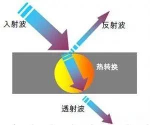
(Figure 1: Propagation Path of Electromagnetic Waves in a Lossy Medium )
FEHONDA Explains the Absorption Mechanisms
FEHONDA's understanding of electromagnetic wave absorption involves key mechanisms:
-
Conductive Particle Interaction: When conductive particles are incorporated into the absorbing material (reaching a certain volume fraction), they can come into contact, forming an electrically conductive network. When an external electromagnetic field encounters this material, the strong EM waves interact with the free electrons within the conductive particles. These free electrons are set into motion, generating their own electromagnetic field that opposes the external field. This opposition leads to the cancellation and weakening of the electromagnetic interference wave.
-
Energy Conversion: Following the principle of energy conservation, when electromagnetic waves strike the free electrons in the conductive particles, the kinetic energy of these moving electrons is converted into heat due to the inherent electrical resistance of the conductive particles. This process effectively transforms the electromagnetic interference wave into thermal energy, leading to its dissipation.
FEHONDA's Innovation: Enhancing Magnetic Absorbing Material Performance through Anisotropy
FEHONDA is actively exploring innovative techniques, such as inducing anisotropy (direction-dependent properties) in magnetic absorbing materials, to further enhance their absorption performance. This tailored approach allows for the development of materials with optimized absorption characteristics for specific frequency ranges and applications.
Evaluating the Effectiveness of Absorbing Materials: FEHONDA's Perspective
From FEHONDA's research standpoint, the fundamental requirements for evaluating the performance of absorbing materials are twofold:
-
Strong Electromagnetic Wave Absorption Capability: The material must effectively absorb a significant portion of the incident EM energy.
-
Wide Frequency Coverage: The material should be effective across a broad range of electromagnetic frequencies.
To quantify the electromagnetic wave absorption capability, FEHONDA and the broader scientific community primarily utilize two key metrics:
-
Reflection Loss (RL): Measured in decibels (dB), RL indicates the power loss of the electromagnetic wave upon reflection from the material's surface at a specific frequency. A more negative RL value signifies better absorption.
-
Effective Absorption Bandwidth: This refers to the frequency range (in GHz) over which the RL is below -10 dB. An RL of -10 dB corresponds to the absorption of 90% of the incident electromagnetic wave energy. A wider effective absorption bandwidth indicates a more versatile absorbing material.
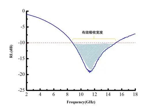
(Figure 2: Electromagnetic Wave Absorption Performance Curve)
Figure 2 illustrates a typical performance curve for an absorbing material. The vertical axis represents the Reflection Loss (RL), and the horizontal axis represents the frequency. The curve depicts how the RL of the material changes with frequency at a specific thickness. Generally, a curve that lies lower on the graph (more negative RL values) and exhibits a wider effective absorption bandwidth indicates superior absorption performance. Intuitively, the larger the area enclosed by the curve and the -10 dB line (the shaded region in the figure), the better the absorption characteristics. Furthermore, the frequency range of the effective absorption bandwidth is also a crucial consideration. While many absorbing materials exhibit absorption peaks in the high-frequency region, a wider and more strategically positioned bandwidth is often desired.
FEHONDA Clarifies the Distinction: Absorbing Materials vs. Electromagnetic Shielding Materials
Absorbing materials often have a counterpart: electromagnetic shielding materials. Understanding the difference between these two is crucial for selecting the appropriate solution for EM mitigation. In simple terms:
-
Absorbing Materials: Aim to completely absorb incident electromagnetic waves, minimizing both reflection and transmission. The EM energy is dissipated within the material.
-
Electromagnetic Shielding Materials: Focus on preventing electromagnetic waves from entering a protected device by reflecting the waves away. The EM energy is redirected, not eliminated.
Therefore, while both types of materials prevent electromagnetic waves from passing through a protected area, their mechanisms of action differ fundamentally: absorption versus reflection. Consequently, the evaluation methods for shielding materials also differ from those used for absorbing materials. The primary metric for evaluating shielding effectiveness (SE) in dB.
FEHONDA: Your Partner in Electromagnetic Wave Management
At FEHONDA, we are committed to advancing the development and application of high-performance electromagnetic wave absorbing materials. Our research focuses on creating innovative solutions that address the growing challenges of EM pollution across various industries. By understanding the fundamental principles of absorption, the methods for evaluating performance, and the distinction between absorbing and shielding materials, we empower our customers to make informed decisions for effective electromagnetic wave management. Stay tuned for FEHONDA's cutting-edge absorbing material solutions designed for a cleaner and more reliable electromagnetic environment.