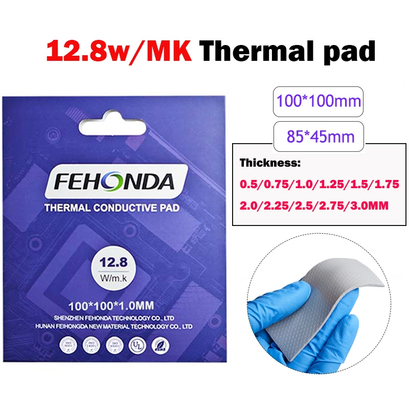
FEHONDA-GPCF350SL
What GPCF3505L is
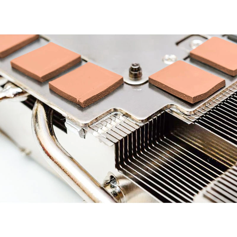
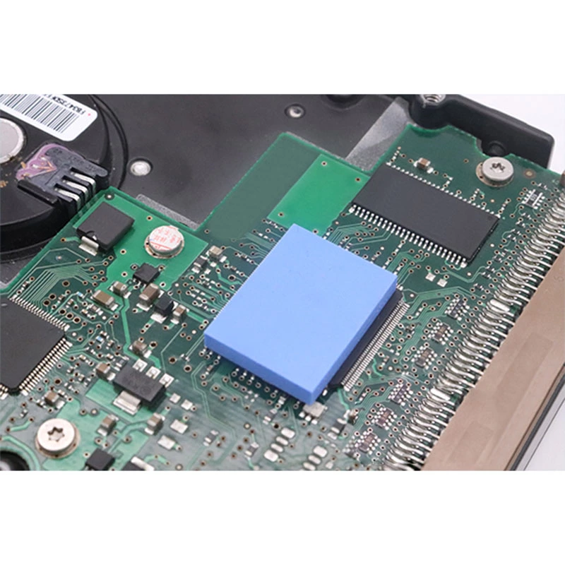
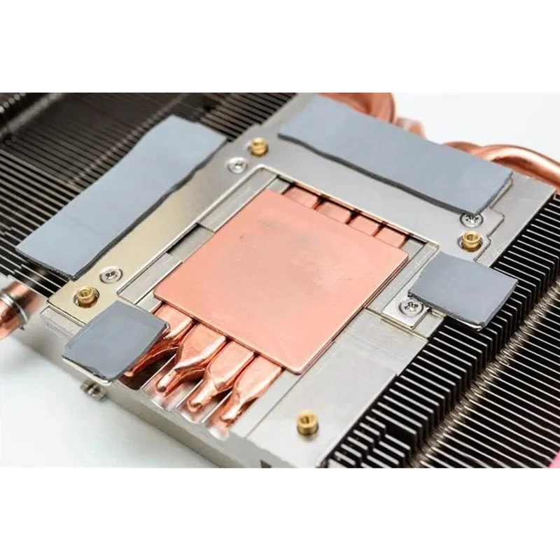
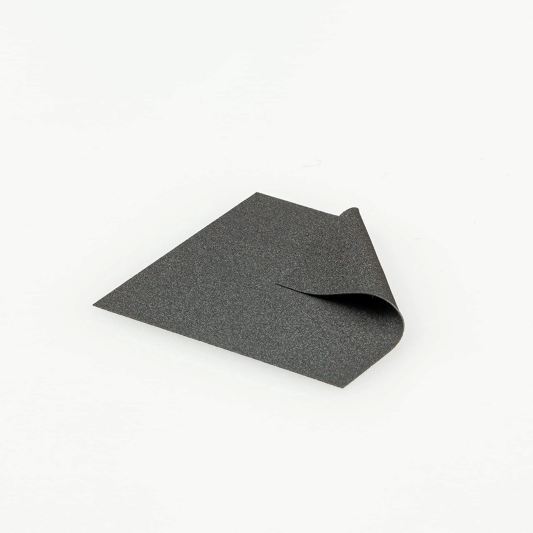
GPCF3505L is a thermally conductive pad built on a liquid silicone rubber base, filled with carbon fibre and nickel-plated graphite. It is supplied as a solid, flexible sheet rather than a grease or a brittle film, and it sits in the contact interface between a heat source and a heat sink, filling the air gaps there so heat can cross.
Four properties define it.
- Thermal conductivity of 35.0 W/(m·K), measured through the thickness of the pad at 1 mm and 20 psi per ASTM D5470.
- Thermal resistance of 0.09 °C·in²/W under the same conditions — the figure that actually predicts how the joint behaves.
- Hardness from Shore 00 40 to 90, so softness can be matched to the application.
- UL94 V-0 flame rating, valid across the full 0.3 to 12 mm thickness range, over a -50 to 160 °C operating window.
Two of those numbers are worth some explanation, because they are the ones that decide whether this is the right part for your interface.
FEHONDA | Product Datasheet Guide
GPCF3505L Carbon Fibre Thermal Pad
35.0 W/(m·K) through-plane, 0.09 °C·in²/W at 1 mm, in a flexible V-0 pad from 0.3 to 12 mm
1.Specification
| Property | Value | How to Test |
| Thermal conductivity | 35.0 W/(m·K), through-plane | Measured per ASTM D5470 at 1 mm and 20 psi |
| Thermal resistance | 0.09 °C·in²/W | At 1 mm and 20 psi per ASTM D5470. About 0.58 °C·cm²/W |
| Hardness | Shore 00 40 to 90 | Shore 00 scale, not Shore A. Select within the range to suit assembly pressure and flatness |
| Colour | Black | Visual |
| Thickness range | 0.3 to 12 mm | Select against the measured gap, as thin as the stack allows |
| Density | 2.6 ± 0.2 g/cm³ | Heavier than a conventional pad; relevant where weight matters |
| Base material | Liquid silicone rubber | Gives flexibility, conformability and compression recovery |
| Filler | Carbon fibre;Alumina | Both are conductive — see the cautions below |
| Flame rating | UL94 V-0 | Valid across the full 0.3 to 12 mm thickness range |
| Operating temperature | -50 to 160 °C | Confirm this is continuous, not a short-term peak |
| Adhesive option | A1 single-sided; A2 double-sided | Where the pad needs to be held in place during assembly |
| Shelf life | 24 months | Store in a ventilated, cool, dry place |
| Packaging | To customer requirement | Supports low-volume and custom orders |
| Compliance | RoHS and REACH passed | supporting test reports |
2.Why through-plane is the number that matters
arbon fibre is highly anisotropic: axial conductivity ≈900–1,100 W/(m·K), radial ≈5–10 W/(m·K) — a ~100× gap. So a carbon-fibre composite has two different conductivities, depending on which way the fibres point.
GPCF350SL's 35.0 W/(m·K) is measured through the thickness — the direction that counts for an interface material, since heat must cross the joint from component to heat sink, not just spread sideways.
The two directions are near-opposites, and through-plane is the harder one to achieve. Calendering — the natural way to form a filled sheet — lays fibres flat, giving high in-plane but poor through-plane. Standing fibres up across the bond line needs a deliberate alignment step (magnetic, electric, flow-field or shear). So a genuinely high through-plane figure tells you about the manufacturing route, not just the formulation — and it explains why many carbon-fibre pads quote an impressive number that does little at the interface.
When comparing suppliers, ask for the direction on the test report. A figure with no direction will be read as through-plane, and finding out otherwise costs a redesign.
| Quantity | °C·in²/W | °C·cm²/W | What it is |
| Ideal material resistance, 1 mm at 35.0 | 0.044 | 0.29 | Thickness divided by conductivity. No contact resistance included |
| Measured, 1 mm at 20 psi, ASTM D5470 | 0.09 | 0.58 | The real joint, including contact resistance at both faces |
| Difference | about 0.046 | about 0.29 | Contact resistance — roughly equal to the material resistance itself |
That difference is the point, and it is not a defect. Contact resistance at the two mating faces accounts for about half the total. Two things follow from it, and both are more useful than the conductivity figure alone.
- Use the resistance, not the conductivity, when you calculate. The 0.09 figure already contains the contact behaviour under a stated pressure, which is exactly what a conductivity number leaves out.
- Surface quality and mounting pressure matter about as much as the material. If half the resistance is at the interface, then flatness, roughness and clamp load are worth roughly as much as the pad you choose. This is why we ask about them before quoting.
One caution on units. The measured value is stated in °C·in²/W, following ASTM D5470 convention.
3.Why thickness still decides the result
A high conductivity figure does not license a thick pad. Thermal resistance rises with bond line no matter how good the material is. The table below shows the idealised material resistance, thickness divided by conductivity, in °C·in²/W. Actual measured values are higher, because they include contact resistance — at 1 mm the measured figure is about twice the ideal, as shown above.
| Bond line | GPCF3505L at 35.0 | A 3.0 W/(m·K) pad | Ratio |
| 0.5 mm | 0.022 | 0.26 | about 12x |
| 1.0 mm | 0.044 | 0.52 | about 12x |
| 3.0 mm | 0.13 | 1.55 | about 12x |
| 5.0 mm | 0.22 | 2.58 | about 12x |
Read it in both directions, because both readings matter.
- Across a row: GPCF3505L is roughly twelve times better than a 3.0 W/(m·K) pad at every thickness. That advantage is real and consistent.
- Down a column: going from 0.5 mm to 5.0 mm multiplies the resistance of the same material by about ten. A good material does not rescue a thick bond line.
So the practical case is specific and worth stating precisely: this material earns its place where the gap is unavoidably thick or uneven and you still need usable thermal resistance.
4.Choosing within the Shore 00 40 to 90 range
The hardness range is wide on purpose, and picking a point in it is a real design decision rather than a default. Shore 00 is the softest durometer scale — note it is not Shore A, which is a different scale and a much harder material. The two are frequently confused on datasheets, and a figure without its scale is not a specification.
| End of range | Behaviour | Best for | Trade-off |
| Shore 00 40 to 60 | Very soft, conforms with little force, wets rough or uneven surfaces | Uneven substrates, low assembly pressure, mixed component heights, delicate packages | Lower resistance to compression set over long service |
| Shore 00 60 to 75 | Balanced | General interface use where flatness is reasonable and pressure is moderate | The default if you have no strong constraint either way |
| Shore 00 75 to 90 | Firmer, holds shape, resists extrusion under high clamp load | High mounting pressure, thin bond lines, automated pick-and-place handling | Needs flatter surfaces and more force to conform |
The useful rule: softer wins wherever the surfaces are imperfect or the pressure is low, because contact beats conductivity — and the measured resistance above shows contact carrying about half the total. Firmer wins where the stack is flat, clamped hard, and the pad has to survive handling on a line. Tell us the flatness and the pressure and we will recommend a point in the range rather than leaving you to guess.
5.What it replaces
GPCF3505L sits in a specific gap in the market. Conventional filled pads are soft and conformable but typically stay below about 10 W/(m·K). Graphite films spread heat superbly across the plane but are brittle, effectively incompressible, and weak through their thickness. A metal spreader plate conducts well but adds weight and cannot absorb tolerance.
A carbon-fibre-filled silicone composite does all three jobs in one layer: high through-plane conductivity, real compressibility, and useful lateral spreading. That is the case for it.
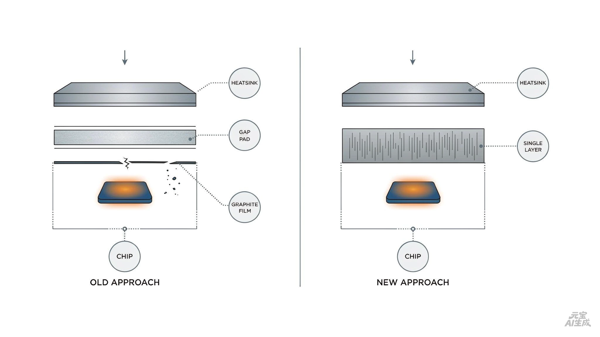
Figure 2. One flexible composite layer in place of a brittle graphite film plus a separate gap pad.
6.Key advantages
- 35.0 W/(m·K) measured through the thickness, at 1 mm and 20 psi per ASTM D5470. The direction that actually moves heat across a joint, achieved by aligning the fibre rather than relying on filler loading alone.
- 0.09 °C·in²/W measured thermal resistance under the same stated conditions, so the number can go straight into a thermal calculation rather than being derived.
- Softness you can specify. Shore 00 40 to 90 means the pad can be matched to the surface and the pressure, instead of forcing the design to suit one hardness.
- Usable resistance where the gap is thick or uneven. No graphite film can serve this situation, and a conventional pad loses roughly a factor of twelve.
- One layer instead of two. Removing a graphite film and a gap pad removes an interface, and interfaces are where thermal resistance accumulates.
- Wide thickness range, 0.3 to 12 mm. Unusually broad, so one material can cover several positions in a design and simplify the bill of materials.
- V-0 across the entire 0.3 to 12 mm range, not just at one tested thickness. That removes a compliance question for designs using several thicknesses.
- Adhesive-backed options. A1 single-sided or A2 double-sided, which removes a lamination step and holds the pad in place during assembly.
- Conductive filler brings shielding and grounding behaviour with it. Where a design needs both, that is a part count and assembly saving — but only if you actually need conductivity. See the cautions.
7.Recommended applications
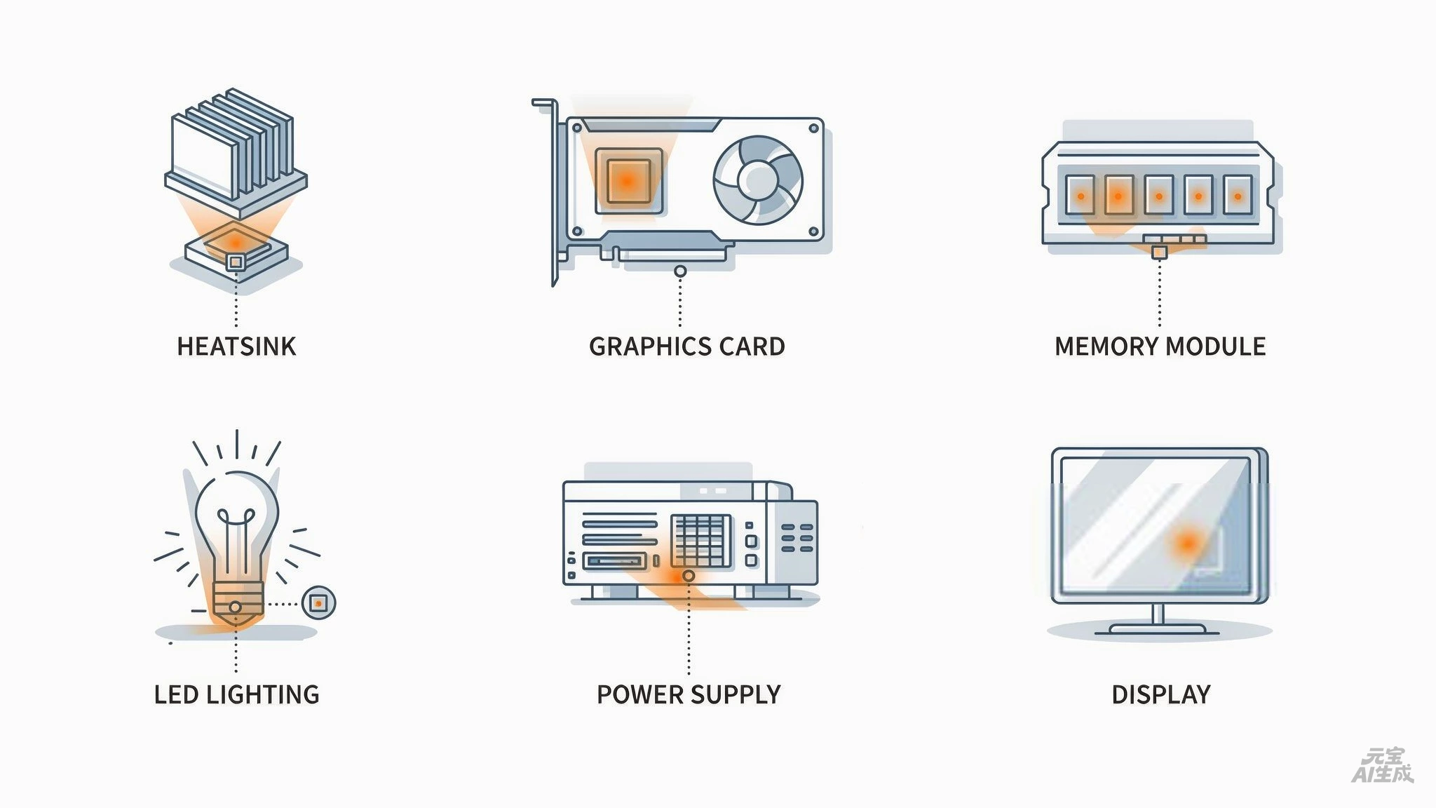
Figure 3. Typical application positions across computing, lighting, communications and display.
| Application | Where it goes | Why this material |
| Semiconductor heat sinks | Between the device and the heat sink or spreader | High through-plane conductivity, with flexibility to absorb flatness and mounting tolerance |
| Automotive navigation units | Processor and power devices to the housing | Compressibility absorbs stack variation; -50 to 160 °C covers in-vehicle extremes |
| Communications power equipment | Power devices to the enclosure wall or chassis | Sustained load plus production tolerance; conductivity and compliance together |
| Graphics cards and memory modules | GPU die, VRAM, VRM and memory packages to the cooler or chassis | Handles mixed component heights and high flux; the thickness range covers several positions in one build |
| LED lighting | LED board to the housing | The housing is the heat sink; V-0 and a wide temperature range suit enclosed luminaires |
| LCD and plasma televisions | Driver and power board to the chassis or rear cover | Spreading helps where airflow is absent, and the material absorbs stack variation |
A useful rule for all six: this material earns its place where the interface is the bottleneck and you also need compliance. If the bottleneck is airflow or heat-sink area instead, a more expensive interface will not move the result much.
8.Two cautions we would rather you heard from us
Both follow from the filler, and both are the kind of thing that surfaces late if nobody mentions them early.
| Caution | Why it matters | What to do |
| The material is electrically conductive | Carbon fibre and nickel-plated graphite both conduct. Comparable nickel-graphite silicone products are specified as conductive and sold for shielding and grounding. Across live tracks, terminals or uninsulated pads, it will bridge them | If you need dielectric strength, use a composite TIM with a reinforced insulating layer, or specify an insulating laminate. Tell us the voltage and creepage requirement and we will tell you whether this is the right part |
| Carbon in contact with aluminium can corrode | Carbon sits at roughly +0.25 V and aluminium at roughly -0.75 V. That is a large potential difference, and in humid or salt-laden conditions the pair forms a strong galvanic cell that pits the aluminium | Keep an insulating barrier between the material and bare aluminium, or use anodised or coated aluminium. This matters most in outdoor, coastal and automotive environments |
Neither is a reason to avoid the material. Both are reasons to place it deliberately, and to tell your supplier what it will be touching.
9.Why FEHONDA
Large material suppliers are built for volume. That is fine if you want ten thousand of one part. It is a poor fit if you are developing, qualifying, or running a product where the thermal design is still moving. This is where a focused manufacturer is genuinely easier to work with.
- Fast sampling and short lead times. We turn prototype pieces around quickly, because we know a thermal decision usually sits on the critical path of a build.
- Small-batch orders accepted. You do not have to commit to production volume to get production-grade material. That matters for pilot runs, low-volume products and spare parts.
- High prototyping responsiveness. Send a revision, get a revised sample. Iterating thickness, hardness or adhesive during development is normal for us, not an exception we charge for.
- Custom manufacture to your drawing. Die-cut shapes from your CAD, thickness matched to your measured gap, hardness selected within the Shore 00 40 to 90 range, colour coding where a build needs several variants told apart on the line, and packaging to your requirement.
- Engineering input before the quote. Tell us the gap range, the mounting pressure, the flatness and what the material will touch, and we will tell you whether this is the right part — including when it is not.
- Test data stated with its conditions. Conductivity at a stated thickness and pressure, thermal resistance per ASTM D5470, and V-0 across the whole thickness range, rather than a bare number with no method behind it.
- RoHS and REACH declarations with supporting test reports, available on request rather than after a chase.
If you are a small or mid-sized team, the practical benefit is simple: you get to talk to the people making the material, and you can change your mind during development without renegotiating a minimum order.
10.Next step
Send us the drawing with the gap range, the mounting pressure, the flatness of the mating surfaces and what the material will be touching. We will come back with a recommendation on hardness and thickness, samples and a lead time. If GPCF3505L is not the right part for your interface, we will say so and point you at the one that is.
Please submit your request via our custom service form to ensure a faster response.
11.Frequently asked questions
Is 35.0 W/(m·K) through the thickness or across the plane?
Through the thickness. That is the direction that matters for an interface part, because heat has to cross the joint to the heat sink rather than spread sideways within the pad. It is also the harder direction to achieve: calendering tends to lay fibres flat, so a high through-plane figure comes from a deliberate alignment step during manufacture. When comparing suppliers, always ask which direction a figure refers to — an unqualified number is usually read as through-plane, and that assumption sometimes fails.
What is the thermal resistance, and under what conditions?
0.09 °C·in²/W, measured at 1 mm and 20 psi per ASTM D5470, which is about 0.58 °C·cm²/W. Note the units: square inches and square centimetres differ by a factor of 6.45, so check which one a supplier quotes before comparing. The value applies at the stated thickness and pressure, so ask us for data at your own conditions if they differ.
Why is the measured resistance higher than the conductivity suggests?
Because the measured figure includes contact resistance at both faces, which the conductivity number does not. At 1 mm the ideal material resistance would be about 0.044 °C·in²/W, and the measured 0.09 is roughly twice that. The practical consequence is that surface flatness, roughness and mounting pressure contribute about as much as the material does, which is why those are worth getting right.
What hardness should I specify?
It depends on flatness and assembly pressure. Toward Shore 00 40 to 60 the pad is very soft and conforms to uneven surfaces under low force, which suits mixed component heights and delicate packages. Toward Shore 00 75 to 90 it is firmer, holds its shape and resists extrusion under high clamp load, but needs flatter surfaces. Around 60 to 75 is a reasonable default when nothing is pushing you either way. Note this is the Shore 00 scale, which is for soft materials — it is not Shore A.
Can I use it where I need electrical insulation?
No, not as supplied. Carbon fibre and nickel-plated graphite are both conductive, and comparable nickel-graphite silicone products are sold specifically for shielding and grounding. Where the interface is also a voltage barrier, use a composite TIM with a reinforced insulating layer, or add an insulating laminate. Tell us the voltage and clearance and we will recommend accordingly.
Does it replace a graphite film?
Sometimes. It replaces a graphite film where you also need to fill a gap, absorb tolerance, or avoid handling a brittle sheet that sheds conductive particles. It is not a straight replacement where your only problem is lateral spreading across a large flat area — graphite film has the much higher in-plane number there, in the order of 1,000 to 1,900 W/(m·K). The honest answer depends on which of those two problems you actually have.
Do I need the adhesive-backed version?
Only if the pad is not mechanically clamped. A1 is single-sided and A2 is double-sided, and either removes a separate lamination step and holds the pad in place during assembly. Where the stack is screwed or clamped under real pressure, the plain pad is usually better, because any adhesive layer adds thermal resistance.
Can I specify a thick pad because the conductivity is high?
No. Thermal resistance rises with bond line, so going from 0.5 mm to 5.0 mm multiplies the material resistance by about ten. The advantage over a conventional pad is about a factor of twelve at any given thickness, but the benefit of a thin bond line still dominates.
What is the shelf life?
24 months when stored in a ventilated, cool, dry place. Packaging is supplied to your requirement, which suits low-volume and custom orders.