1. Why GPU thermal management became a system-level problem
GPUs did not simply get hotter — the shape of the thermal problem changed. Four shifts matter most when you are choosing a material:
- Sustained load, not burst load. A gaming GPU spikes for a few seconds and then idles. An AI accelerator holds every streaming multiprocessor at close to 100% utilisation for weeks. There is no recovery window for the interface to relax, so creep, pump-out and dry-out all accelerate.
- Heat is concentrated, not spread. Hotspots on advanced AI dies reach 100–500 W/cm² while the surrounding silicon runs far cooler. A healthy average temperature can hide a local hotspot that trips the throttle.
- Throttling is paid twice. A GPU that drops its clock to protect itself is paid for once in hardware and again in lost FLOPs. Across a training cluster, a few degrees of junction temperature translates directly into longer time-to-model.
- Liquid cooling changed the material requirements. Once a board meets a cold plate or is immersed in dielectric fluid, the TIM must also survive coolant contact, thermal cycling and package warpage. Low volatility and low oil bleed stop being nice-to-have and become qualification criteria.
2. Where the heat actually gets stuck: the GPU thermal path
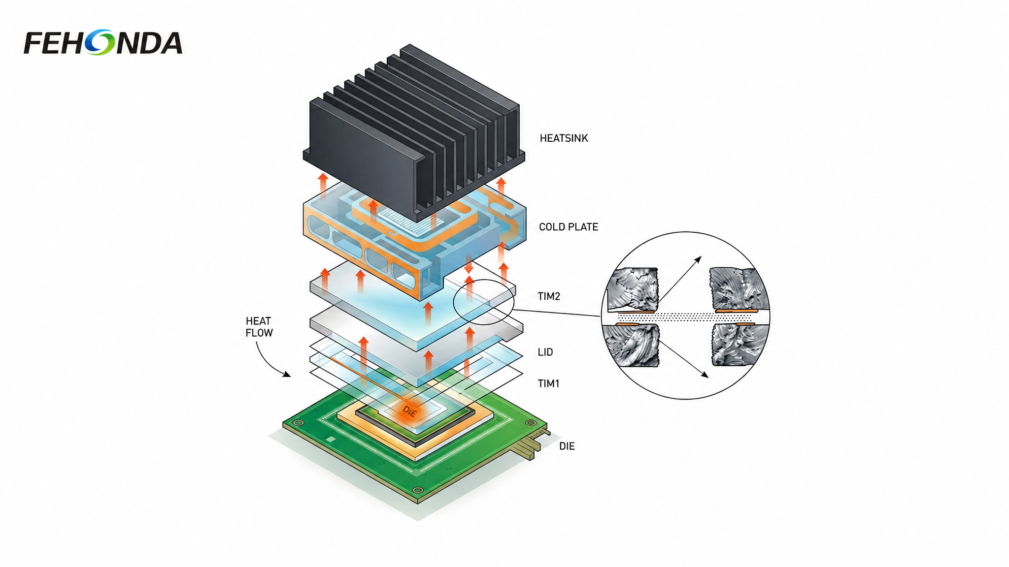
Every GPU cooling solution — air or liquid — is a chain of thermal resistances in series. Heat leaves the junction and crosses the following layers before it reaches the ambient:
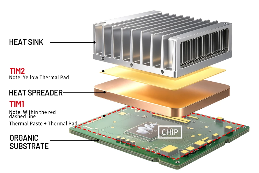
Figure 1. The GPU thermal path. Two of these layers, TIM1 and TIM2, are the only ones a materials supplier controls
3. The four mainstream polymer TIM families
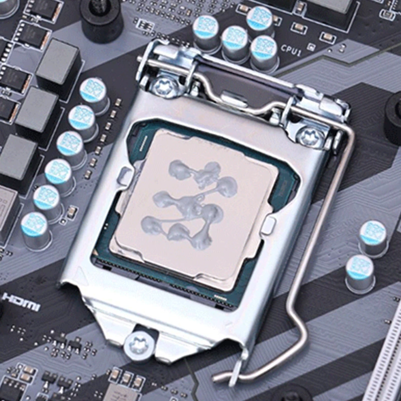
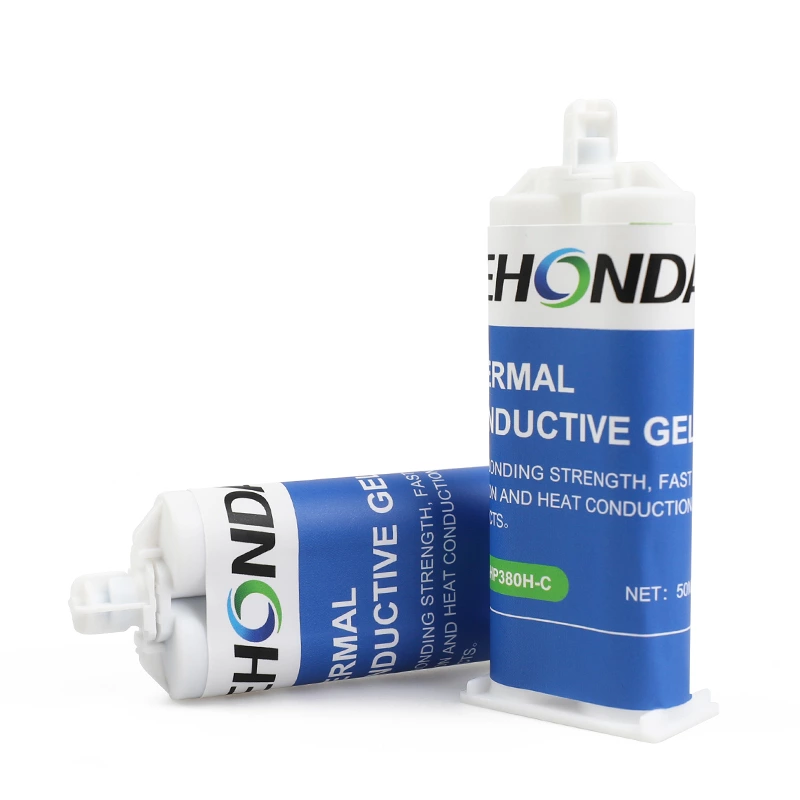
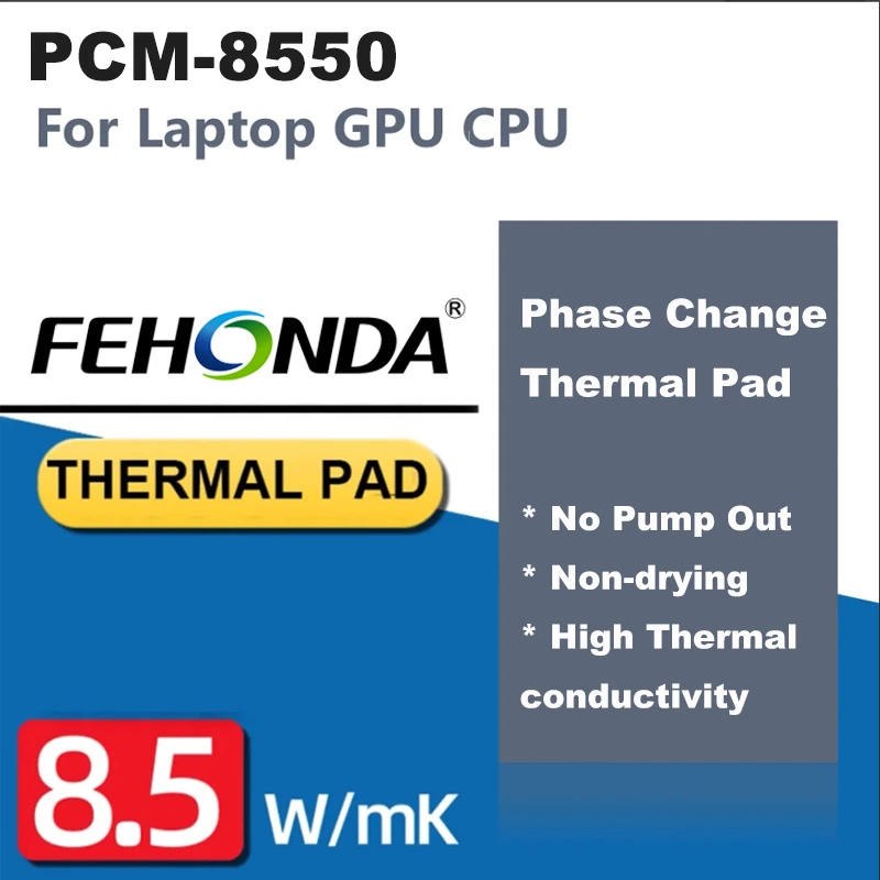
Polymer-based products — silicone or non-silicone matrices filled with ceramic or metal-oxide powder — account for roughly 70–80% of the global TIM market, because they balance performance, processability and cost. The ranges below are typical industry figures for the category; always confirm against the specific datasheet.
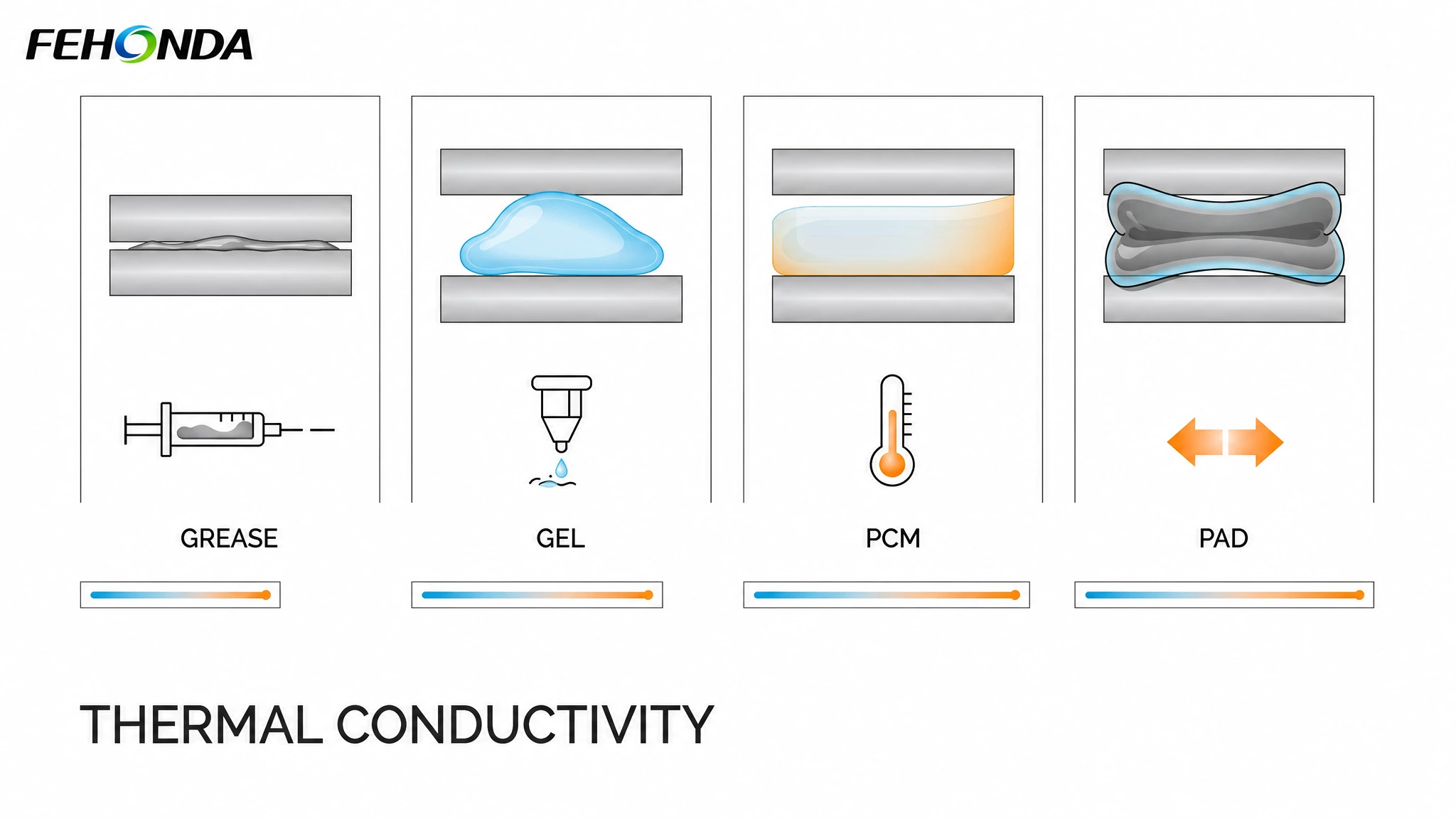
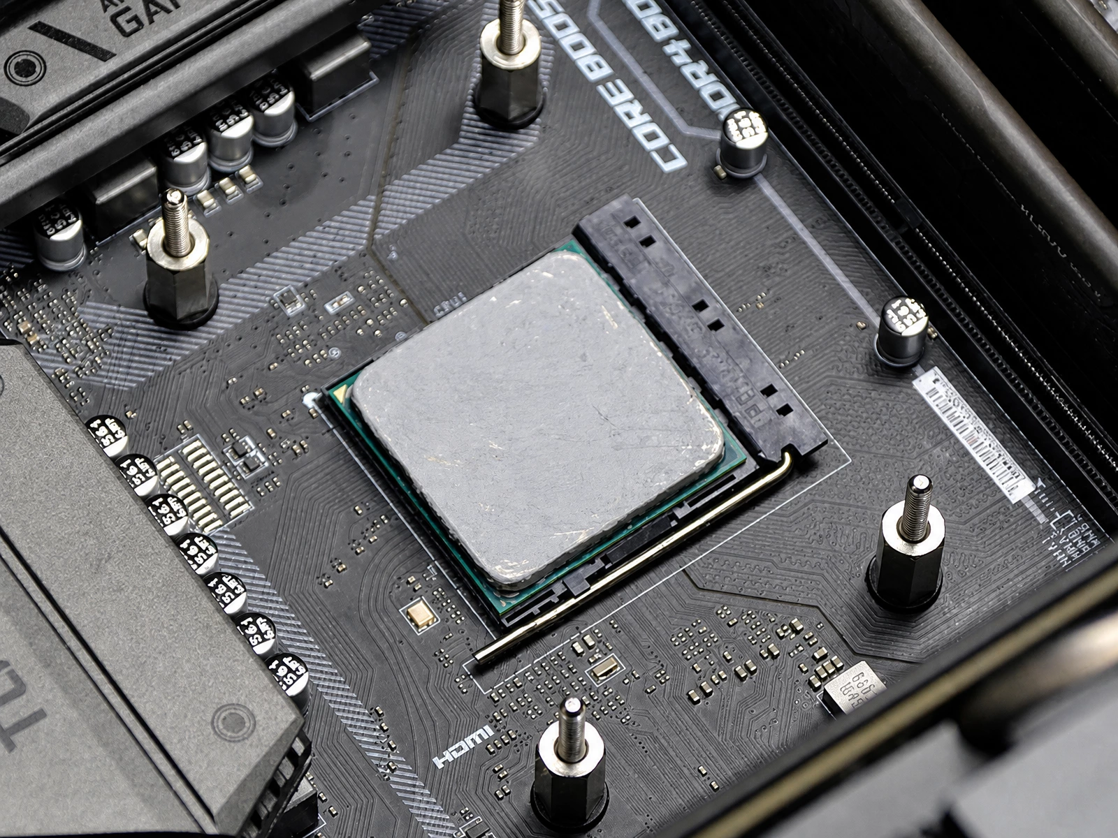
Figure 2. The four mainstream polymer TIM families. Bond line thickness and assembly method usually matter more than peak conductivity.
| Family |
Conductivity |
Bond line |
Assembly |
Best fit on a GPU |
| Thermal grease |
1–8.5 W/(m·K) |
0.05–0.06 mm |
Dispense / print |
Thin, flat, high-flux interfaces; rework-friendly but prone to pump-out |
| Thermal gel / gap filler |
1–8 W/(m·K) |
0.10–0.22 mm |
Automated dispensing |
Irregular gaps, VRM and memory arrays, high-volume liquid-cooled assembly |
| Phase-change material |
3–8.5 W/(m·K) |
0.13–0.50 mm |
Place, then heat activate |
Long-service servers; lower pump-out risk than grease, clean handling |
| Thermal pad |
1–16 W/(m·K) |
0.3–10.0 mm |
Pick and place |
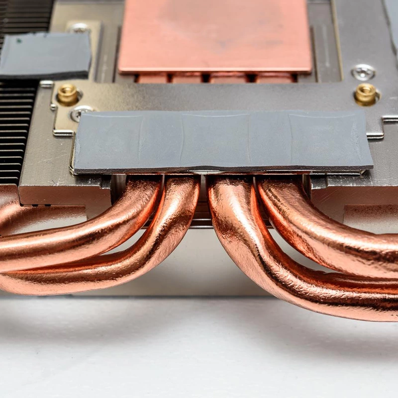
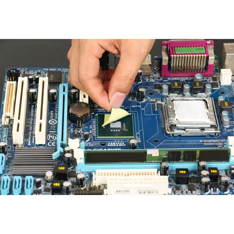
Large or variable gaps, electrical isolation, field-serviceable modules |
Two notes on reading that table. First, thermal resistance is the number that reaches the junction temperature, not conductivity — a pad's contact resistance is strongly pressure-dependent and can fall sharply once it is properly compressed. Second, a thin bond line of a modest material usually outperforms a thick bond line of an excellent one, which is why dispensable gels have displaced pads in many high-volume cold-plate builds.
4. A four-step framework for selecting a GPU TIM
Work through these questions in order. Each one eliminates options before you reach the datasheet, which keeps the selection fast and defensible.
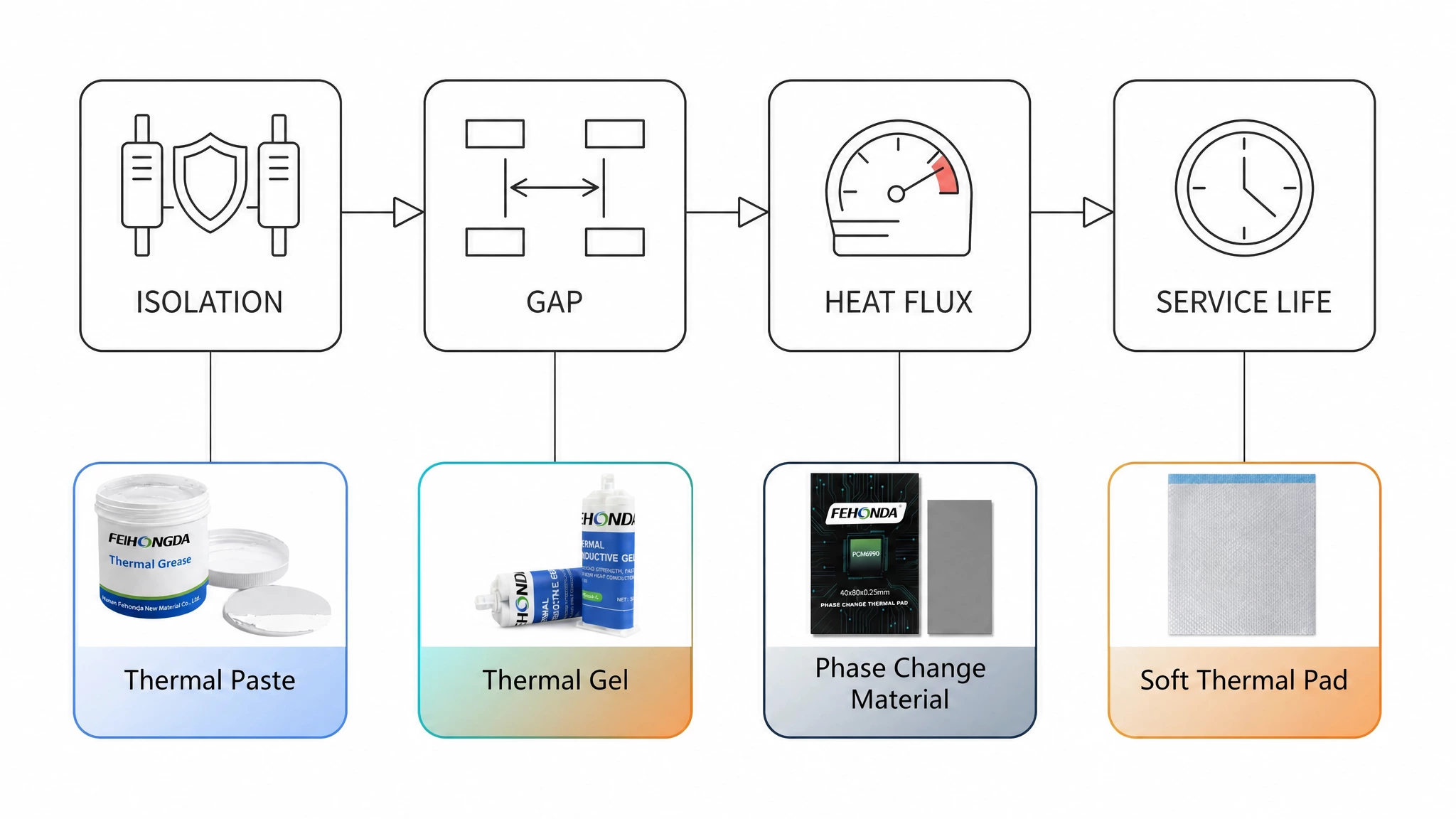
Figure 3. Selection sequence: isolation, gap, heat flux, then service life.
- Step 1 — Is electrical isolation required? If the interface must insulate, start with a pad or a filled gel and confirm dielectric strength. If it does not, high-conductivity greases and metal-based options remain on the table.
- Step 2 — What is the real gap? Measure the tolerance stack-up across the whole mating area, not at one point. Under roughly 100 µm, look at grease or phase-change. Between 100 and 500 µm, pads and gels compete. Beyond 500 µm, a dispensable gap filler is usually the only practical answer.
- Step 3 — What is the heat flux? Below about 50 W/cm² most polymer options are comfortable. Above that, move to high-conductivity grease, phase-change or a metal-based interface, and revisit the mounting pressure.
- Step 4 — How long must it last, and can it be reworked? Five-year data-centre service with no maintenance favours phase-change and cured gels. Field-serviceable or rework-heavy builds favour pads. Short-life consumer cards can accept grease.
5. Where TIM is applied on a GPU board and inside an AI server
A GPU assembly rarely has a single thermal interface. The die is the headline, but memory, power stages and structural interfaces all need material — and they usually need different materials:
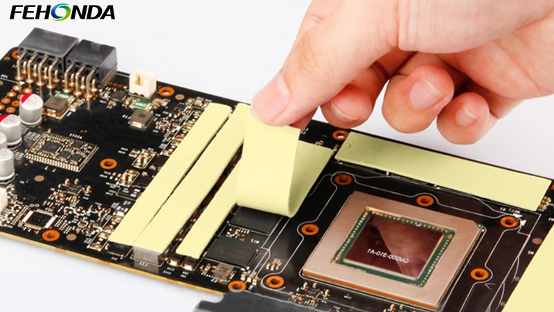
Figure 4. Typical thermal interface material application points on a graphics card and an AI server GPU module.
- GPU die / package lid — the highest-flux interface. Thin bond line, lowest achievable contact resistance.
- Memory (HBM / GDDR) — a ring of lower-height chips around the die. Needs a compliant material that bridges a height difference without excessive pressure.
- VRM and power stage — MOSFETs and drivers run hot and are height-mismatched to the die. Gel or pad, chosen for gap coverage rather than peak conductivity.
- Inductors and regulators — moderate heat, larger gaps, often the reason a pad thickness range is selected rather than a single value.
- Cold plate / structural interface — large area, tight flatness tolerance. This is where dispensable gel and automation compatibility pay back in assembly yield.
6. How thermal performance is actually measured: ASTM D5470
Conductivity figures are only comparable when you know the method behind them. ASTM D5470 is the most widely cited steady-state standard for thermally conductive electrical insulation materials, and it is the method most TIM datasheets reference.
The principle is straightforward: a specimen of known thickness is clamped between two isothermal parallel surfaces, a temperature gradient is imposed, and the resulting one-dimensional heat flow is measured once steady state is reached. Four consequences matter to a specifier:
- It measures thermal impedance, not conductivity directly. Conductivity is then derived, which is why the standard uses the term apparent thermal conductivity — these filled polymers are heterogeneous, not homogeneous solids.
- It classifies materials by mechanical behaviour. Type I covers viscous liquids that deform without limit — greases, pastes and phase-change compounds. Type II covers viscoelastic solids such as gels and soft rubbers. Type III covers elastic solids such as ceramics and metals.
- Contact resistance must be removed, not ignored. The standard measures impedance at several thicknesses; the inverse slope of impedance versus thickness gives apparent conductivity, and the intercept at zero thickness is the fixture contact resistance. A single-thickness measurement therefore overstates impedance and understates conductivity.
- Test conditions are part of the result. Surface finish and parallelism are specified, and the applied pressure and bond line thickness must be quoted. A material reported at 10 psi and 200 µm is not comparable to one reported at 40 psi and 60 µm — and a datasheet that omits both should be treated as incomplete.
When you compare two materials, ask for three numbers together: apparent thermal conductivity, thermal impedance, and the pressure and bond line thickness at which both were measured. Those three, plus the test method, are what make a comparison meaningful.
7. Frequently asked questions
What thermal conductivity do I need for a GPU?
For the die-side interface on a high-power accelerator, start at 6 W/(m·K) and above and prioritise contact resistance over conductivity. For secondary interfaces such as memory, VRM and cold-plate coupling, 1.5–6.0 W/(m·K) is the usual working range, and gap coverage matters more than the headline number.
Is a higher W/(m·K) rating always better?
No. Total thermal resistance is what sets junction temperature, and it depends on both conductivity and bond line thickness. A lower-conductivity material applied at half the thickness will often outperform a higher-conductivity one that has to bridge a larger gap.
Thermal paste or thermal pad — which should I use on a GPU?
Paste wins where the gap is very thin and flat and the flux is high. Pads win where the gap is large or variable, where electrical isolation is required, and where the module must be reworked in the field. Many production GPU boards use both, in different locations.
How long does thermal interface material last in a data centre?
Well-specified cured gels and phase-change materials are normally qualified for five years or more of continuous service. Uncured grease in a thermally cycled assembly is the shortest-lived option, which is why pump-out testing is part of AI server qualification.
Why does my datasheet quote ASTM D5470?
Because it is the recognised steady-state method for measuring thermal impedance and deriving apparent conductivity across greases, gels, phase-change compounds and pads. It provides a common baseline — provided the pressure and bond line thickness are reported alongside the result.
8. Next step
FEHONDA supplies thermal potting compounds, thermally conductive silica and thermally conductive gels for power electronics, energy storage and high-power computing, with conductivity grades spanning 1.5 to 18.0 W/(m·K) characterised under ASTM D5470. Our sales and engineering support teams can help with grade selection, dispensing trials, coolant compatibility checks and product customisation.
Send us your stack-up — gap range, mounting pressure, target junction temperature and service profile — and we will come back with a shortlist and sample recommendations.
📩 Contact our technical team: sales@fehonda.com